Successful cases
PCB Line Width Detection
Application Scenario
With the increasing demands in PCB manufacturing for finer apertures, smaller pitches, and higher speeds, the line width and spacing on circuit boards have reached the micron level. This requires more precise and efficient visual inspection solutions to ensure product quality.
Project Challenges
1. High Line Density: High-precision PCBs have dense routing, with the minimum line width on bare boards as small as 1 mil. Manual inspection struggles to identify such fine details, compromising the reliability of quality assurance.
2. High-Speed Production Lines: The fast pace of industrial production lines necessitates rapid inspection speeds.
3. Defect Visibility: Issues such as scorching and yellowing of the PCB, oxidation of copper traces, and uneven color require color imaging to accurately detect and restore the appearance of various defects.
I-TEK Solution: 16K Color Line Scan Camera (PR16KCXP10-40KC)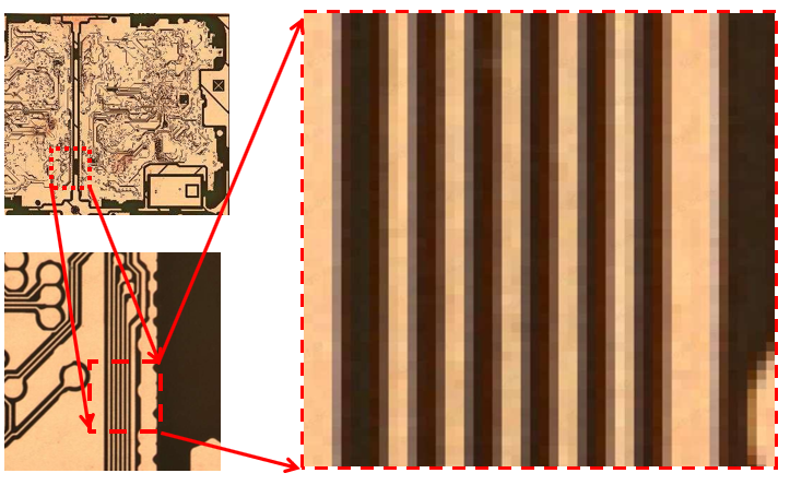
PR16KCXP10-40KC Imaging Performance
1. High-Resolution Imaging: As shown in the image above, the I-TEK 16K color line scan camera, with a resolution of 16,384 x 6 and a 5 x 5μm pixel size, meets the demands for wide-field, high-precision inspection of 2 mil PCBs.
2. High Line Rate: The camera supports a maximum line rate of 40 kHz and employs TDI (Time Delay Integration) technology, significantly enhancing sensitivity. It also features a CoaXPress10 interface, achieving a data rate of up to 1900 MB/s, ensuring high responsiveness and a wide dynamic range, even during high-speed production line operations.
3. Advanced Color Correction: I-TEK's advanced color space correction technology ensures excellent color reproduction, accurately restoring potential defects such as surface flaws, contamination, and color inconsistencies on the product.