Successful cases
Wafer Inspection
Application Scenario
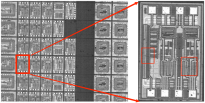
Wafer manufacturing involves creating circuits and embedding electronic components (such as transistors, capacitors, logic gates, etc.) on the wafer, making it one of the most technically complex and capital-intensive processes.
I-TEK Solution: 65MP High-Speed Area Scan Camera
This solution enables precise inspection of the wafer's appearance, circuitry, and critical dimensions, ensuring that all types of defects are clearly visible.
Inspection Results