Successful cases
Semiconductor Packaging Inspection
Application Scenario
Packaging is mainly completed in the later stages of semiconductor manufacturing. It involves using film technology and fine connection technology to arrange, fix, and connect semiconductor components and other elements on a frame or substrate, leading to the formation of the main structure by encapsulating the components with a plastic insulating medium.
Project Challenges
With advancements in chip packaging technology, the pin grid spacing is getting smaller, and pin density is increasing, posing higher demands on visual inspection systems.
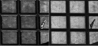
I-TEK Solution: 8K Multi-Exposure Time Division Flash Strobe Line Scan Camera
This solution utilizes bright and dark field contrast to inspect wafer dicing, wire bonding, trimming, molding, and character printing.
Inspection Results